

-
The “Electronics Kit” Common Emitter Amp
Posted on August 20th, 2017 No commentsOne project that’s been in my mind for ages is to revisit some of the circuits from my childhood Philips X40 kit. I finally got around to putting “Experiment 5 – Telephone pick-up and amplifier” in to my circuit simulator. This is the first of several audio amplifier circuits in the manual, and they all follow the same design pattern. Similar circuits are also used in other educational kits. I had tried to use this circuit design in my own electronics experiments as a kid. Mostly it didn’t work, but sometimes it did. As an adult, I was interested to understand its characteristics to help explain where it’s appropriate.
View the about in full screen.
Looking at the simulation you will notice the amplifier is non-linear (compare the shape of the top of the sine wave out to the bottom in the output of the first stage). This isn’t unexpected given that transistors have an exponential relationship between the base voltage and the collector current. The biasing on the second stage also looks bad, meaning that the output signal is clipped on the positive side. The simulation result raises several questions in my mind:
- Why is this type of amplifier so popular in basic electronic kits?
- Are they circumstances in which the amplifier is linear?
- What are the characteristics of this type of amplifier anyway?
To answer these questions, let’s look at the basic building block of this amp. It’s a single transistor common emitter configuration. The biasing is from a high value resistor between the collector and the base. Wikipedia informs me that this configuration is called “collector feedback bias“. The signal is coupled in and out of the stage through capacitors.
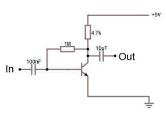
Single Stage of Amplifier
Looking at this circuit you can guess why it’s popular in these kits: the component count is very low. Hence, it is easy for kids to build. If you have an intuitive understanding of transistors, you might also guess that resistor between the collector and the base creates negative feedback giving the circuit the ability to find a suitable operating point across a range of conditions.
As all the textbooks tell you, transistor amplifiers require that the transistor(s) are “biased” correctly to work. The aim of biasing is to set the DC conditions around the transistor so that it is in the “active zone” of operation. The active zone means that you are past the threshold for the base voltage required to start to turn the transistor on, but not yet at the base voltage where the transistor is fully turned on and saturated. The DC conditions that the biasing establishes are called the “operating point”.
As I mentioned, in this circuit the base resistor provides negative feedback which tends to stabilize the operating point. When the circuit is switched on there is no current through the transistor so the collector voltage is at the power supply voltage and the base is pulled high though the two resistors. This rising base voltage turns the transistor on and this pulls the collector voltage down (because of a voltage drop through the collector resistor) which in turn reduces the base voltage – tending to turn the transistor off and reduce the collector current. In practice, these effects will almost instantaneously reach equilibrium with the transistor in a partially on state – i.e. in its active region.
Wikipedia gives a pretty good explanation of how to calculate the operating point so I won’t repeat it. One thing to note though, for the resistor values used in this configuration, the operating point will depend on the gain (β) of the transistor so the operating point will change for different transistors. Here is a graph showing how Vc depends on the gain (β).
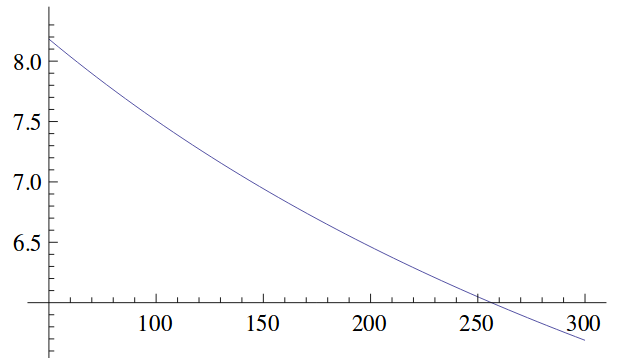
Theoretical Vc (Y axis) Vs Gain (X axis) for Circuit Shown Above
So, that just about wraps-up the situation for the DC bias. It works just about OK as long as you aren’t fussy and don’t expect a big output voltage swing I guess! What about the AC characteristics of this circuit? What is the gain? What about this non-linearity effect?
I checked a few standard text books, and the web, and couldn’t find a theoretical treatment for this circuit configuration so I had to come up with my own. Let’s start by assuming that the impedance of the input source through the coupling resistor is low compared to the input impedance of the amplifier. In that case the input signal becomes just a change in voltage on the base of the transistor (ΔVBE). In that case we can use the Ebers-Moll equation for the transistor to work out the impact on the collector current (and hence the collector voltage). Ebers-Moll says:
IC2/IC1 = Exp( ΔVBE / VT ) Where VT ≈ 25.3mV at room temperature
If you write IC2 = IC1 + ΔIC, and convert the collector current to the corresponding voltage you can get the solution:
ΔVC = ( 1 – Exp( ΔVBE / VT) ) . ( VCC – VC1 )
Where VCC is the power supply voltage and VC1 is the voltage at the collector at the quiescent operating point
That equation fascinates me for two reasons:
- Clearly, this is an exponential amplifier – which explains the non-linearity
- The gain depends on the collector voltage at the quiescent operating point. The graph above which shows how the operating point changes with β translates to changes in the stage gain.
Can we imagine this amp could be approximately linear? Well, as my high-school physics teacher said “everything is linear if you look at a small enough range” (cue sound of 1,000,000 mathematicians groaning). So, we know by Taylor expansion that:
Exp( x ) = 1 + x + x2/2! + x3/3! + …
So, if ΔVBE << VT we can approximate the exponential using just the first two terms above.
ΔVC ≈ – ( ΔVBE ) . ( VCC – VC1 ) / VT
In other words, for very small input signals (<< 25mV) it is kind-of, sort-of, a linear amplifier of gain ( VCC – VC1 ) / VT . Here are some handy plots from Mathics of gain Vs β, Rc and Rb.
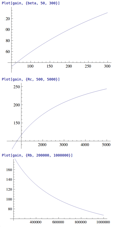
Stage Gain (Y axis) Vs β (Top), Rc (Middle), Rb (Bottom)
Actually, the stage gain in this configuration is quite high, though very dependent on the β of the transistor. I might also remark that the output impedance is poor (limited by Rc ), though, without having done the calculation, I think the input impedance is probably OK.
So, if you want a high gain, single stage, small signal amp with very few components, and, you aren’t too worried about predictability of the gain OR linearity OR output impedance then this circuit just about does the job. This actually fits the bill for these beginner’s electronic kits pretty well. If your requirements are more stringent then better avoid this circuit and look for others. Just one thing still seems odd – why is the second stage bias set where it is on the original circuit?
For me it’s been interesting to look at how much information you can extract about this, fairly trivial, circuit and it’s certainly refreshed my understanding of transistor fundamentals. I hope you find it interesting too.